The École Polytechnique Fédérale de Lausanne (EPFL, France) claims to have repaired severed spinal cord injuries in rats, and is planning to adapt the technology for use in humans. The new method encourages the nerves to grow back, giving hope to those who may be able to restore lost functionality after a spinal injury: R. Colin Johnson
Here is that EPFL says about restoring spinal cord injuries: Rats with spinal cord injuries and severe paralysis are now walking (and running) thanks to researchers at EPFL. Published in the June 1, 2012 issue of Science, the results show that a severed section of the spinal cord can make a comeback when its own innate intelligence and regenerative capacity—what lead author Grégoire Courtine of EPFL calls the "spinal brain"—is awakened. The study, begun five years ago at the University of Zurich, points to a profound change in our understanding of the central nervous system. It is yet unclear if similar rehabilitation techniques could work for humans, but the observed nerve growth hints at new methods for treating paralysis.
Further Reading
Thursday, May 31, 2012
#WIRELESS #ENERGY: "Recharging Just Got Automatic"
Most of us have to lug along a different wall wart for each wireless device we want to recharge, but an emerging standard interface will soon allow a common station to recharge all. The Wireless Power Consortium's Qi standard promises to enable any smartphone, tablet, digital camera or similar rechargeable mobile devices to use the same wireless recharging stations--just set your device on the black pad and it automatically recharges through the air inductively: R. Colin Johnson

Wireless rechargers cut the last cord to tablets by recharging merely by lying then on a specially wired surface. Source: Freescale Semiconductor
Here is what EETimes says about wireless recharging:Wireless inductive battery rechargers already cut the cable to many devices such as electric toothbrushes, but because there were no standards in place until recently, they still require a proprietary recharge station. Now that the Wireless Power Consortium has over 100 members for its Qi standard, analysts predict the time is ripe for a global wireless charging market, which is expected to exceed 100 million units annually by 2015, according to IMS Research (Austin, Texas).
Further Reading
Wednesday, May 30, 2012
#WIRELESS: "Industrial Apps go Multi-Platform"
The hyper-text mark language version five (HTML5) is capable of creating apps that run identically on different platforms enabling independent software developers (ISVs) to spend their time writing new code rather that rewriting for different operating systems. By creating an HTML-engine for each smartphone and tablet OS, Motorola Solutions can now offer its software app developers the ability to cut their development efforts while fully supporting bring-your-own-device (BYOD) trends in the modern enterprise: R. Colin Johnson

Motorola's Enterprise Tablet (ET1) used by businesses like HomeDepot for sales personnel can now run the same HTML5 apps as front-office users on their iPad, Blackberry Playbook or Windows 8 tablet.
Here is what EETimes says about HTML5 apps: Those ruggedized Motorola Solutions' ET-1 tablets you see point-of-sale clerks at Home Depot and elsewhere wielding to display product features, scan barcodes and take credit cards are also being used in the warehouse to manage inventory and by buyers to visualize their entire supply chain. In the front office, however, ruggedized tablets are unnecessary, prompting Motorola Solutions to craft RhoMobile Suite, a software development environment for Windows PCs or MacOS computers that churns out universal HTML5-based apps that run not only one Motorolas ruggedized ET-1, but also on smartphones and tablets.
Further Reading
#NANOTECH: "Tiny Giraffe Sculpture Wins Science as Art Contest"
The world's smallest giraffe sculpture has won the Science as Art contest at the 2012 Materials Research Society spring meeting. The "found art" was just 50 microns in size and handpainted (in Photoshop) to bring out the giraffe's natural colors: R. Colin Johnson
Here is what University of California at Riverside says about its nano-giraffe: Shaahin Amini was ready to quit. The Ph.D. student at the University of California, Riverside’s Bourns College of Engineering had spent three hours looking into a microscope scanning a maze of black-and-white crosshatched lines, tubes and beads made of nickel, aluminum and carbon magnified 3,800 times.
Then he saw it. It looked like some kind of animal. He zoomed in further. It now looked like the road runner from the Bugs Bunny cartoons. He rotated it. Bingo! A sheep? No, a giraffe. A 0.05 millimeter giraffe.
He spent a few hours using Photoshop to add brown for the skin patches, red for the tongue and green in the background to resemble a jungle. It was done.
He submitted the piece to the Science as Art competition at 2012 MRS (Materials Research Society) Spring Meeting in San Francisco. Amini’s piece, which was one of about 150 entries, was selected by the chairs of the meeting as one of the 50 finalists from throughout the world to be displayed in the exhibition hall. Meeting attendees voted on the winners and selected Amini’s piece as one of the first-place winners.
Amini is a fourth-year Ph.D. student working with Reza Abbaschian, dean of the Bourns College of Engineering and William R. Johnson, Jr. Family Professor of Engineering.
Amini’s research area is the nucleation and growth kinetics of graphene layers from molten metals. Graphene is a single-atom thick carbon crystal with unique properties, including superior electrical and heat conductivities, mechanical strength and unique optical absorption, which could have widespread use in electronics. Amini, for the first time, developed a novel processing technique to grow single layer graphene from a molten phase.
The feature that Amini turned into a giraffe was created during the melting process of nickel, aluminum and carbon mixture. As the molten alloy solidified, the nickel and aluminum formed the body of the giraffe while the carbon was rejected and crystallized as a graphite cover. After further cooling, the graphitic cover wrinkled, due to less contraction than the metallic substrate, created a network of creases resembling the familiar skin patches of a giraffe.
Further Reading
#WIRELESS: "Graphene Tooth Tattoo Detects Bacteria"
Wireless 'tooth tattoos' may soon be used to detects harmful bacteria in the mouth. By combining a super sensitive grapheme sensing array with a small antenna, a handheld device can pick up signals from the tooth tattoo allowing maladies to be diagnosed with a remote reader: R. Colin Johnson

The sensor, shown here on a cow's tooth, detects bacteria in the body and passes a signal to a nearby receiver. (Photo by Michael McAlpine)
Here is what Princeton says about its tooth tattoo: Using silk strands pulled from cocoons and gold wires thinner than a spider's web, researchers at Princeton University have created a removable tattoo that adheres to dental enamel and could eventually monitor a patient's health with unprecedented sensitivity.
In a laboratory in Princeton's Engineering Quadrangle, a graduate student demonstrated the system's wireless capability, breathing across a sensor attached to a cow's tooth. Instantaneously, the sensor generated a response to the student's breath and transmitted a signal to a nearby monitor.
The researchers created the tattoo by bundling the silk and gold with graphene — an extremely thin sheet of carbon in which atoms are arranged in a honeycomb lattice. The material's unique properties allowed the researchers to construct a small, flexible device able to detect bacteria at a much higher sensitivity level than traditional methods. In tests, the researchers detected samples of bacteria that can cause surgical infections and others that can lead to stomach ulcers.
By combining the graphene array with a small antenna, the detection can be picked up by a remote reader device that is small enough to be held in a user's hand
The results were reported March 27 in the journal Nature Communications. In addition to professor Michael McAlpine, the paper's authors included graduate student Manu Mannoor, undergraduate Jefferson Clayton, Assistant Professor of Electrical Engineering Naveen Verma and associate research scholar Amartya Sengupta at Princeton; Hu Tao, David Kaplan and Fiorenzo Omenetto of Tufts University; and Rajesh Naik, of the Air Force Research Laboratory. Support for the research was provided by the American Asthma Foundation and the Air Force Office of Scientific Research.
To build the devices, McAlpine's team first imprinted tiny graphene sensors onto an extremely thin film of water-soluble silk. (The Tufts researchers pulled silk strands from cocoons, dissolved them in a solution and dried the mixture to create the silk base.)
Next, the researchers made an antenna by depositing a pattern of thin gold strands onto the silk film, and connected it to the graphene sensors. When completed, the device resembles a common removable tattoo. To attach the sensor, the researchers place it against a tooth, or a person's skin, and wash it with water. The silk base dissolves in the water, but the graphene sensor and the antenna remain securely fastened to the spot.
To allow the device to detect certain types of bacteria, the researchers attached peptides — fragments of proteins — to the graphene sensors. The peptides bind to bacterial cells and allow the researchers to detect a signal change from the graphene sensors.
McAlpine said one of the goals was to create a device that was small, flexible and passive, capable of providing detection from within the body or other remote location. So the researchers designed the device without a power supply. Instead, an external radio transmitter held nearby the device delivers a signal that causes the device to
Designing the antenna was one of the project's challenges. The gold coil needs to be big enough to transmit a readable signal, but small enough to fit within the sensor's compact footprint. The team was able to attach the current version of the system to a cow's tooth; reducing the size of the sensor in order to fit onto a human's tooth would require further work.
The current design allows for detection at a relatively short but practical distance, roughly a centimeter. Verma said if longer range was needed for other applications, modifications could be developed for the system.
The researchers said one of the key developments of the research was the use of graphene with a biocompatible base, in this case silk. Current biosensors tend to be relatively rigid and heavy, and they are often uncomfortable for patients. In large part, that is a result of sensors' base material, called a substrate.
In addition to its flexibility and biocompatibility, the solubility of silk meant that it could wash away with water or be dissolved by the body's enzymes.
The team plans to conduct further studies to better understand the adhesion between the tooth enamel and the graphene sensor with the goal of achieving a longer-lasting bond and enhancing the longevity of the system. One of the challenges for a dental system is protecting the sensor from inadvertent damage from things like brushing.
Further Reading
#MATERIALS: "Schrödinger's Hat Aims to Amplify Matter"
Everyone after Einstein knew that matter is really waves, that electrons for instance have a wavelength that causes quantum properties to emerge when they are confined is a space smaller than their wavelength. Now researchers are proposing to amplify, filter and otherwise manipulate such matter waves using a meta-material-based device. Called a Schrödinger's hat, it performs signal processing on matter waves while remaining invisible to outsiders : R. Colin Johnson

A matter wave hitting a Schrodinger's hat. The wave inside the container is magnified. Outside, the waves wrap as if they had never encountered any obstacle. Credit: G. Uhlmann, U. of Washington
Here is what the University of Washington says about matter waves: Invisibility, once the subject of magic or legend, is slowly becoming reality. Over the past five years mathematicians and other scientists have been working on devices that enable invisibility cloaks – perhaps not yet concealing Harry Potter, but at least shielding small objects from detection by microwaves or sound waves.
A University of Washington mathematician is part of an international team working to understand invisibility and extend its possible applications. The group has now devised an amplifier that can boost light, sound or other waves while hiding them inside an invisible container.
As a first application, the researchers propose manipulating matter waves, which are the mathematical description of particles in quantum mechanics. The researchers envision building a quantum microscope that could capture quantum waves, the waves of the nanoworld. A quantum microscope could, for example, be used to monitor electronic processes on computer chips.
The authors dubbed their system "Schrödinger's hat," referring to the famed Schrödinger's cat in quantum mechanics. The name is also a nod to the ability to create something from what appears to be nothing.
Gunther Uhlmann, who is on leave at the University of California, Irvine, has been working on invisibility with fellow mathematicians Allan Greenleaf at the University of Rochester, Yaroslav Kurylev at University College London in the U.K., and Matti Lassas at the University of Helsinki in Finland, all of whom are co-authors on the new paper.
The team helped develop the original mathematics to formulate cloaks, which must be realized using a class of engineered materials, dubbed metamaterials, that bend waves so that it appears as if there was no object in their path. The international team in 2007 devised wormholes in which waves disappear in one place and pop up somewhere else.
For this paper, they teamed up with co-author Ulf Leonhardt, a physicist at the University of St. Andrews in Scotland and author on one of the first papers on invisibility.
Recent progress suggests that a Schrodinger’s hat could, in fact, be built for some types of waves.
The research was funded by the National Science Foundation in the U.S., the Engineering and Physical Sciences Research Council and the Royal Society in the U.K., and the Academy of Finland.
Further Reading
Tuesday, May 29, 2012
#SECURITY: "Flame Malware Attacking Iran"
Yet more state-sponsored malware has been found attacking Iran and other anti-west regimes in the MiddleEast, according to Kaspersky Lab. The newest malware, called Flame, appears to be smarter than previous attack suites--Stuxnet and DuQu--in that it does not spread randomly, which allowed Flame to remain undetected for at least two years: R. Colin Johnson

Here is what Kaspersky says about Flame: Kaspersky Lab announces the discovery of a highly sophisticated malicious program that is actively being used as a cyber weapon attacking entities in several countries. The complexity and functionality of the newly discovered malicious program exceed those of all other cyber menaces known to date.
The malware was discovered by Kaspersky Lab’s experts during an investigation prompted by the International Telecommunication Union (ITU). The malicious program, detected as Worm.Win32.Flame by Kaspersky Lab’s security products, is designed to carry out cyber espionage. It can steal valuable information, including but not limited to computer display contents, information about targeted systems, stored files, contact data and even audio conversations.
The independent research was initiated by ITU and Kaspersky Lab after a series of incidents with another, still unknown, destructive malware program – codenamed Wiper – which deleted data on a number of computers in the Western Asia region. This particular malware is yet to be discovered, but during the analysis of these incidents, Kaspersky Lab’s experts, in coordination with ITU, came across a new type of malware, now known as Flame. Preliminary findings indicate that this malware has been “in the wild” for more than two years - since March 2010. Due to its extreme complexity, plus the targeted nature of the attacks, no security software detected it.
Although the features of Flame differ compared with those of previous notable cyber weapons such as Duqu and Stuxnet, the geography of attacks, use of specific software vulnerabilities, and the fact that only selected computers are being targeted all indicate that Flame belongs to the same category of super-cyberweapons.
Commenting on uncovering Flame, Eugene Kaspersky, CEO and co-founder of Kaspersky Lab, said: “The risk of cyber warfare has been one of the most serious topics in the field of information security for several years now. Stuxnet and Duqu belonged to a single chain of attacks, which raised cyberwar-related concerns worldwide. The Flame malware looks to be another phase in this war, and it’s important to understand that such cyber weapons can easily be used against any country. Unlike with conventional warfare, the more developed countries are actually the most vulnerable in this case.”
The primary purpose of Flame appears to be cyber espionage, by stealing information from infected machines. Such information is then sent to a network of command-and-control servers located in many different parts of the world. The diverse nature of the stolen information, which can include documents, screenshots, audio recordings and interception of network traffic, makes it one of the most advanced and complete attack-toolkits ever discovered. The exact infection vector has still to be revealed, but it is already clear that Flame has the ability to replicate over a local network using several methods, including the same printer vulnerability and USB infection method exploited by Stuxnet.
Alexander Gostev, Chief Security Expert at Kaspersky Lab, commented: “The preliminary findings of the research, conducted upon an urgent request from ITU, confirm the highly targeted nature of this malicious program. One of the most alarming facts is that the Flame cyber-attack campaign is currently in its active phase, and its operator is consistently surveilling infected systems, collecting information and targeting new systems to accomplish its unknown goals.”
Kaspersky Lab’s experts are currently conducting deeper analysis of Flame. Over the coming days a series of blog posts will reveal more details of the new threat as they become known. For now what is known is that it consists of multiple modules and is made up of several megabytes of executable code in total - making it around 20 times larger than Stuxnet, meaning that analysing this cyber weapon requires a large team of top-tier security experts and reverse engineers with vast experience in the cyber defence field.
ITU will use the ITU-IMPACT network, consisting of 142 countries and several industry players, including Kaspersky Lab, to alert governments and the technical community about this cyber threat, and to expedite the technical analysis.
Further Reading
#WIRELESS: "15 Surprising (or not) Facts About Texting"
Online College Courses has published the results of what it calls a "scholarly study" into the facts about texting. Its report, “15 Surprising, Scholarly Facts About Text Messaging” breaks a few stereotypes and confirms a few; for instance, testers use fewer abbriviations than you might have thought, but texting while driving really is very dangerous: R. Colin Johnson

Here are the 15 facts about texting (click "further reading" below to read about each one):
• Getting a text makes you happier
• Hypertexters are less healthy
• Texting behind the wheel is even riskier than we thought
• Texting while driving killed 16,000 in a six-year period
• Texters use fewer abbreviations than we thought
• Black people send the most text messages
• Texting helps HIV sufferers take their meds
• Texters don't believe that's a word
• Texting makes it easier to lie
• Many people are addicted to texting
• Most people still prefer a phone call
• Banning texting while driving is not the answer
• Female teens text the most
• Texting has spawned its own injury
• Predictive texting changes children's brains:
Further Reading
#ROBOTICS: "Robotic Jellyfish to Patrol, Cleanse Ocean"
Robotic jellyfish aim to harness one of nature's simplest and most efficient mechanisms to create schools of autonomous vehicles to patrol our oceans. Virginia Tech's robotic jellyfish could be used to patrol for contamination as well as clean up oil spills and other environmental pollutants: R. Colin Johnson

Alex Villanueva and the experimental robotic jellyfish that one day could could patrol the seas for the military and for environmental safeguard.
Here is what Virginia Tech says about their robot jellyfish: Virginia Tech College of Engineering researchers are working on a multi-university, nationwide project for the U.S. Navy that one day will put life-like autonomous robot jellyfish in waters around the world.
The main focus of the program is to understand the fundamentals of propulsion mechanisms utilized by nature. Future uses of the robot jellyfish could include conducting military surveillance, cleaning oil spills, and monitoring the environment.
This isn’t science fiction. It’s happening now in a lab inside Virginia Tech’s Durham Hall, where a 600-gallon tank is regularly filled with water as small robotic jellyfish are tested for movement and energy self-creation and usage. A synthetic rubbery skin, squishy in one’s hand, mimics the sleek jellyfish skin and is placed over a bowl-shaped device covered in electronics. When moving, they look weirdly alive.
The idea for a robotic jellyfish did not originate at Virginia Tech, but rather the U.S. Naval Undersea Warfare Center and the Office of Naval Research. Virginia Tech, is teaming with four U.S. universities on the multi-year, $5 million project: University of Texas at Dallas is handling nanotechnology based actuators and sensors; Providence College in Rhode Island is handling biological studies, University of California, Los Angeles, is handling electrostatic and optical sensing/controls, and Stanford University is overseeing chemical and pressure sensing. Virginia Tech is building the jellyfish body models, integrating fluid mechanics and developing control systems. Several other major U.S. universities and industries also are on the project, as well as collaborators and advisory board members.
The project has been in the works for nearly four years now and has garnered much attention form media outlets from The Los Angeles Times to Popular Science to New Scientist and several marine-related trade publications. Several more years of work remain on the project before any models are released for military reconnaissance or object-tracking operations, be it with cameras, sensors, or other devices.
The smaller models are being developed to be powered by hydrogen, naturally abundant in water, which is a huge step in autonomous craft. The larger models may be operated by electric batteries built into the robotic creature. In both cases, the jellyfish must be able to operate on their own for months or longer at a time as engineers likely won’t be able to capture and repair the robots, or replace power sources.
Further Reading
#MEMS: "Air-Bag Substitutes for Dorky Bike Helmet"
Tired of that dorky bike helmet? Now thanks to micro-electro-mechanical system (MEMS) chips from ST Microelectronics an air-bag for-the-head can replace the ubiquitous helmet, resulting in a stylish look that also offers better protection, according to their inventor Hövding. Upon impact, the air-bag inflates around the head and neck to provide protection against impacts in the ground or nearby objects: R. Colin Johnson
Here is what ST Microelectronics says about invisible bike helmets: Motion sensors and microcontrollers from STMicroelectronics, a global semiconductor leader serving customers across the spectrum of electronics applications, form the brain and senses of the airbag bicycle helmet invented by Hövding, a Swedish design house. The combination of innovative design and state-of-the-art electronics has produced market-unique safety equipment for cyclists in a novel form factor.
International studies show that bicycle helmets reduce injuries by at least 60%. Four in 10 people who die in cycling accidents would have survived had they been wearing a helmet. Despite these alarming statistics, the vast majority of cyclists do not wear helmets for different reasons: they find them bulky, impractical to carry around, or unflattering to wear[1].
The Hövding gear addresses both the safety and practical aspects of bicycle helmets. Unlike traditional skull shells, the ‘invisible‘helmet is a collar worn around the neck with an airbag folded inside. In an accident, ST’s motion sensors pick up the abnormal movements of a cyclist and send a signal to the airbag, which inflates in a tenth of a second to form a hood that surrounds and protects nearly all of the cyclist’s head and neck, while leaving the field of vision open.
The integrated sensors in the collar detect both linear and angular motion in all three dimensions and recognize complex movements of the user with outstanding precision and speed. To determine an accident condition, the sensor system uses sophisticated algorithms defined from a database of specific movement patterns recorded during hundreds of simulated-accident and normal cycling situations.
The electronics in the Hövding helmet are managed by an STM32 microcontroller - a powerful, flexible and reliable control chip that makes sure everything functions reliably and on a minimal energy budget. Among the industry’s largest ARM Cortex M-based microcontroller families, ST’s STM32 comprises more than 300 devices with many different memory configurations, an extensive set of peripherals, outstanding power consumption, and the industry’s best development ecosystem.
The Hövding helmets conform to EU safety regulations (CE-marked) and can be bought in Europe through www.hovding.com
For further information on the Hövding helmets please see videos on http://www.hovding.com/en/film/
Further Reading
Friday, May 25, 2012
#MEMS: "Smart Tennis Rackets Leverage Embedded Sensors"
Tennis appears to the next sport to be enhanced with micro-elecro-mechanical systems (MEMS). These next-generation smart tennis rackets use embedded MEMS sensors and a built-in display to analyze play, improve performance and share experiences with other tennis players: R. Colin Johnson
Here is what Movea says about its selection as the MEMS technology for Babolat's smart tennis racket: Movea (www.movea.com), the leader in motion processing and data fusion technologies, has been selected as technology partner by Babolat, the leading tennis equipment manufacturer, in a groundbreaking effort to develop the racquet of the future.
The “Babolat Play & Connect” racquet will be the first-ever MEMS (Micro Electro-Mechanical Systems) technology enabled racquet with the built-in ability to gather and analyse game data and provide information that could only be manually estimated until now. The “Babolat Play & Connect” racquet will leverage Movea’s integrated SmartMotion® data fusion technology to measure specific elements of a player’s technique, enabling new opportunities for performance analysis, improvement and social results sharing.
Babolat unveiled and demonstrated the first “Babolat Play & Connect” racquet prototype today at the Roland-Garros French Open in Paris and is expected to launch the exciting new product in 2013.
Further Reading
Thursday, May 24, 2012
#MATERIALS: "SRC clears path to 14-nm with directed self-assembly"
The big problem with extending down to smaller chip dimensions is that the features are smaller than the wavelength of the light used to for their lithography, leading to ragged edges and misshaped geometries that engineers have to fix with trial-and-error methods. The cool thing about directed self assembly is that you can use lithography at scales where the wavelength of light is not a problem, then depend on the self-assembling polymers to provide the super-small details with razor sharp edges and atomically perfect geometries: R. Colin Johnson

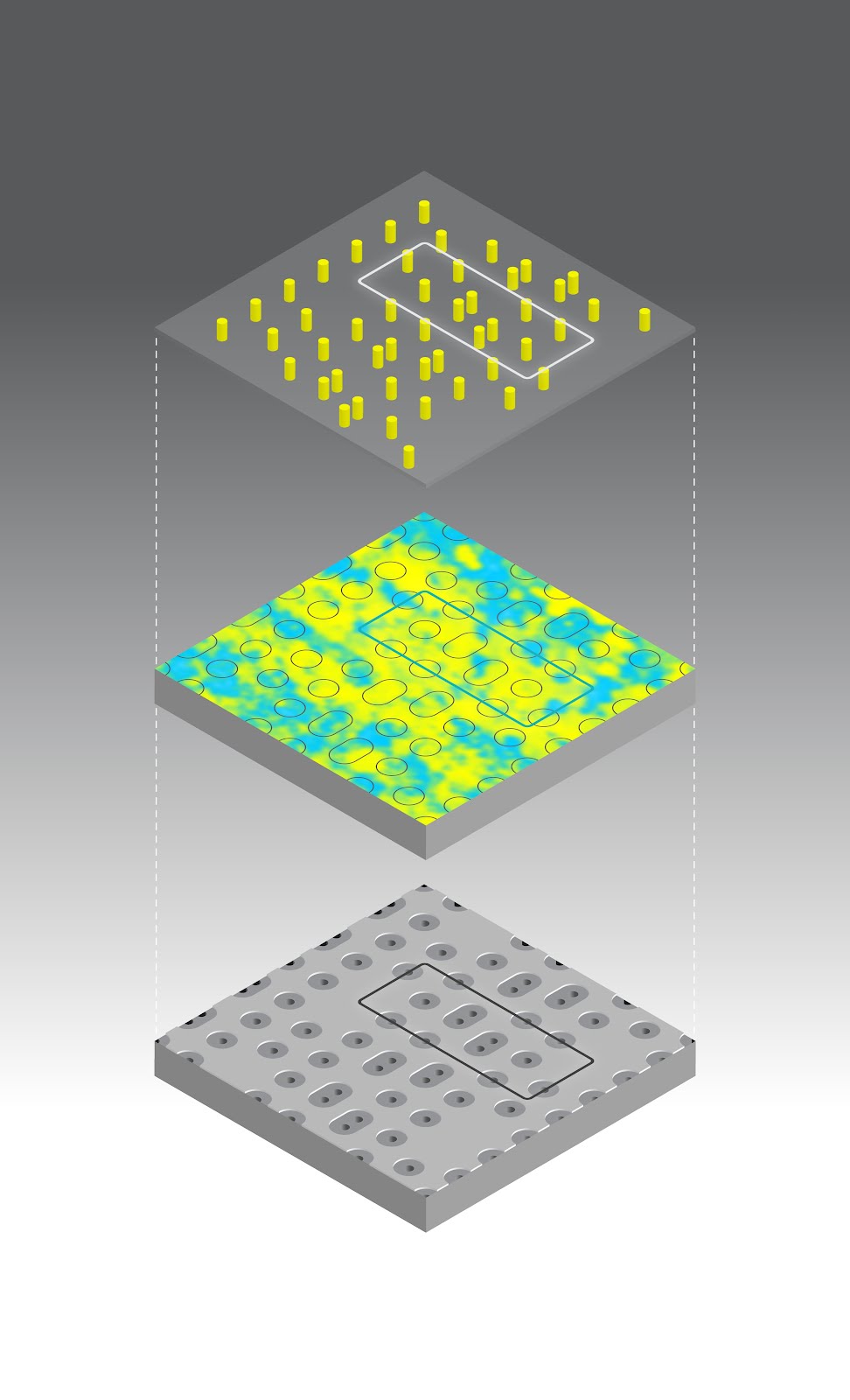
Here researchers demonstrate the contact hole layout for a 22-nm SRAM (top), using a guiding template created with conventional lithography (middle) resulting in the application of a block copolymer to self-assemble the circuit's contact pattern (bottom).
SOURCE: Stanford University
Here is what EETimes says about directed self assembly: A novel self-assembly technique previously demonstrated only in the lab for regular test patterns, has been perfected for creating the irregular patterns necessary to fabricate real semiconductors down to 14-nanometers, according to researchers funded by Semiconductor Research Corp. (SRC).
By solving one of the outstanding lithographic problems facing further scaling—the tiny contact holes that connect semiconductors to their substrate—researchers at Stanford University have demonstrated working circuits at 22-nanometer and a clear path to 14-nanometers, as well as a bee-line on the chemistry developments needed to scale to single digit sizes.
Further Reading
#MEMS "High-G Accelerometer Detects Concussions"
Concussions are a silent epidemic in the U.S. because most of the time they go undiagnosed until the brain has swollen enough to cause symptoms indicating that the damage has already been done. However, by putting a tiny high-G MEMS accelerometer in an ear-plug, any athlete can now monitor whether they received a concussion and get preventative medical help to stop the brain swelling before any damage is done: R. Colin Johnson

IndyCar drivers use these ear-buds to measure head trauma during crashes, each of which has three single axis accelerometers inside. By switching to ADI's new single-chip high-G accelerometer, the next-generation will be three-times smaller, looking more like ordinary ear-plugs. IndyCar's will still have a cord, because the also have a speaker for the radio to the pits, but for NFL and other athletes, instead of a cord, they will just have a red light which illuminates whenever the athlete has received a head shock strong enough to cause a concussion.
Here is what EETimes says about preventing concussions with MEMS: Sports-related concussions have skyrocketed in the U.S. with over 3.8 million reported each year. New MEMS sensors small enough to be mounted inside an athlete's helmet, for example, could perform early detection of symptoms, giving doctors time to administer preventative therapies.
Using high-G sensors for early detection of concussions could drastically reduce injuries, according to the American Association of Neurological Surgeons, since most injuries occur because treatment is delayed. More than 75 percent of concussions go undiagnosed, eventually contributing to over 30 percent of head trauma deaths in the U.S., according to the Centers for Disease Control and Prevention. Early detection also could cut medical bills and lost productivity, which is estimated to exceed $76 billion annually.
Further Reading
#MEMS: "Bosch Combines Gyro + Accelerometer"
Frank Melzer, Bosch Sensortec CEO, announces today the integration into a single inexpensive 3.5-by-4.5 millimeter package a combo accelerometer + gyroscope chip at the MEMS Business Forum in Santa Clara, Calif. Bosch hopes that its manufacturing muscle will persuade mass market smartphone and tablet makers to adopt its six-axis combo inertial measurement unit (IMU) to save board space. Invensense already has a complete nine-axis inertial navigation unit (INU) that includes a AKM magnetometer along with its own six-axis combo chip with accelerometer+ gyro (IMU). However, mainstream smartphone and tablets like Apple's iPhone and iPad still use a separate AKM magnetometer along with separate accelerometer and gyroscope chips coming from volume manufacturer STMicroelectronics: R. Colin Johnson

Bosch 3D chip stack wire bonds its MEMS die with an ASIC holding electronics into a single package.
Here is what EETimes says about IMUs: Inertial measurement units (IMUs) integrate a three-axis accelerometer and a three-axis gyroscope, which Bosch Sensortec now claims to have put into the smallest package yet available for consumer-grade applications such as mobile phones, tablets and digital cameras.
Every smartphone today has a three-axis accelerometer to track motion—for automatically switching its screen from portrait to landscape—but for advanced gaming, gesture recognition and indoor navigational tasks, a three-axis gyroscope is needed, too. Accelerometers only track linear motion, but gyroscopes track rotation-in-place motion, thus providing a higher precision when tracking fine user movements. Packing both accelerometers and gyroscopes into a 3.5-by-4.5 millimeter package could enable any smartphone can upgrade to a full six-degree-of-freedom inertial measurement unit (IMU).
Further Reading
Wednesday, May 23, 2012
#MEMS: "Sensors In Drivers Ears Makes Sunday's Indy 500 to be Safest Yet"
This weekend’s Indy 500 (May 27) could be one of the safest in U.S. auto racing history by combining 200-mph race cars with emerging MEMS technologies.

Along with new safety features created by IndyCar engineers, MEMS sensors like the three high-G accelerometers inside each driver’s earpiece will be used to detect concussions. The same high-G sensors may eventually be used by NASA to protect astronauts from hard splashdowns.

IndyCars are now equipped to stream data from three high-G accelerometers into black-box accident recorders looping through a 90-second memory. In an accident, the system shuts down on impact. After a crash, accelerometer data from 30 seconds before and 60 seconds after impact are correlated with head injuries. Accident data can then be used to improve IndyCar cockpit safety.
Further Reading
Tuesday, May 22, 2012
#CHIPS: "Every 15 Seconds Another Counterfeit Threatens"
A counterfeit part threatens the security of our military and civilian electronic systems every 15 seconds, according to IHS iSuppli. When you count obsolete parts rebranded to appear up to date, the the U.S. is number one with China in second place. Counterfeit parts are especially troubling to the defense and aerospace industries where obsolete parts can cause catastrophic failures: R. Colin Johnson

Countries Where Counterfeit Incidents Were Reported in 2011 (Percentage of Worldwide Total) Source: IHS iSuppli
Here is what IHS iSuppli says about counterfeit parts: More than 12 million parts have been involved in counterfeit incidents during the period spanning the start of 2007 through April 2012, according to Rory King, director, supply chain product marketing at IHS, citing data from ERAI. King delivered the news here on Friday to an audience of electronics industry participants attending the ERAI Executive Conference, co-hosted by IHS.
In his presentation, King noted that reported incidents of counterfeited parts amounted to 1,363 in 2011. However, each incident can include thousands of separate parts, adding up to 12 million over the past five-and-one-quarter years. This equates to slightly more than 1 counterfeit part every 15 seconds.
While the rise in semiconductor counterfeiting is often laid at the feet of China, King noted that the country actually is not the location where most counterfeits are reported.
While the U.S. and China dominate in terms of reports at a combined 65 percent, the countries of origin accounting for the counterfeit parts is more disparate, with the four nations of Malaysia, South Korea, Japan and the Philippines collectively accounting for 64 percent of reports, according to ERAI data. However, the accuracy and value of this data is limited, King noted, given that counterfeiters are highly skilled at disguising the true origin of their wares.
For many companies, particularly those in the defense and aerospace industries, much of the counterfeit risk lies in obsolete parts.
King’s presentation also highlighted the international impact of new U.S. Department of Defense (DoD) regulations on foreign suppliers to the U.S. government. The U.S. National Defense Authorization Act (NDAA), which was signed into law on Dec. 31, imposes strict regulations and severe criminal penalties on counterfeits supplied for government military and aerospace programs.
Further Reading
#MARKETS: "IBM CEO Survey Endorses Personalizing Communications"
IBM'S bi-annual C-Suite study is out. Based on face-to-face conversations with more than 1,700 chief executive officers in 64 countries, IBM's study claims that CEO's are embracing connectedness, empowering employees through values, engaging customers as individuals, amplifying innovation with partnerships, and leading in the connected era by using technology to connect on a more personal level, to erase the constraints of time and distance, and to explore, engage, and expand personal and professional connectedness: R. Colin Johnson

Here is what IBM's C-Suite study says in its executive summary (click :"Further Reading" to download the entire study: For some time now, businesses have been refining and optimizing their networks of suppliers and partners. They’re streamlining supply chains, creating massive back-office efficiencies and perfecting everything from just-in-time inventory to predictive merchandising. But something just as meaningful has been happening in the marketplace — the sudden convergence of the digital, social and mobile spheres — connecting customers, employees and partners in new ways to organizations and to each other. These changes put pressure on the front office to digitize and adapt but also create opportunities for the organization to innovate and lead.
Leaders are recognizing that our new connected era is fundamentally changing how people engage. This shift is one reason why, for the first time since this CEO Study series began in 2004, technology now tops the list of external forces impacting organizations. Above any other external factor — even the economy — CEOs expect technology to drive the most change in their organizations over the next three to five years.
CEOs have a new strategy in the unending war for talent. They are creating more open and collaborative cultures — encouraging employees to connect, learn from each other and thrive in a world of rapid change. Collaboration is the number-one trait CEOs are seeking in their employees, with 75 percent of CEOs calling it critical.
The emphasis on openness and collaboration is even higher among outperforming organizations — and they have the change-management capabilities to make it happen.2 As CEOs open up their organizations, they are not inviting chaos. The need for control remains, but it is evolving into a new form — one better suited to the complexity and pace of business today.
To engage customers as individuals, CEOs are building analytical muscle to respond with relevance and immediacy. As a group, CEOs are investing in customer insights more than any other functional area — far above operations, competitive intelligence, financial analysis and even risk management. More than 70 percent of CEOs are seeking a better understanding of individual customer needs and improved responsiveness. Given the need for deep customer insight, outperformers have a distinct advantage. They are far more adept at converting data into insights, and insights into action. Although face-to-face will remain the most prevalent form of customer interaction, CEOs expect a step-change in the use of social media. Over half expect social channels to be a primary way of engaging customers within five years.
Extensive partnering is providing the edge CEOs need to take on radical innovation. The pressure to innovate is not subsiding, and organizations are teaming to meet the challenge. More than half of all CEOs are partnering extensively to drive innovation. Compared to their less successful peers, outperformers are partnering for innovation more aggressively. But they are also tackling more challenging and disruptive types of innovation. Instead of settling for simply creating new products or implementing more efficient operations, they’re more likely to be moving into other industries or even inventing entirely new ones...To steer their organizations effectively, CEOs told us three leadership traits are most critical: inspirational leadership, customer obsession and leadership teaming across the C-suite. Interestingly, these characteristics closely align with the goals of empowering employees through values, engaging customers as individuals and amplifying innovation with partnerships. This linkage illustrates what CEOs intuitively know: their evolution as leaders directly impacts their organizations’ behavior, culture and, ultimately, results.
Further Reading
#MEMS: "HD Ear Buds for Music and Phone to Allow Conversations Too"
People wearing headsets may soon become even more common, now that STMicroelectronics has teamed with Soundchip to create a single-chip high-definition audio component designed for in-ear monitors. IEMs are designed to be worn all the time, because they pass through sound from the outside world, but can instantly switch to answer your phone or to listen to music. Commercial products are not available yet, but when they are you are likely to know it right away when you see people conversing with each other without removing their ear-buds: R. Colin Johnson

Here is STMicroelectronics says about its MEMS microphone in the Soundchip: STMicroelectronics (NYSE: STM), a global semiconductor leader serving customers across the spectrum of electronics applications and a leading supplier of high-performance audio ICs, together with Soundchip SA, a Swiss-based innovator in audio-systems technology and originator of the High Definition Personal-Audio™ (HD-PA®) Reference, today introduced technologies and components for the smart audio accessory – an exciting new concept in personal listening.
Worn like a pair of In-Ear Monitors (IEMs), the smart audio accessory features new means of controlling and personalizing the sound experience. Designed to be worn at all times, the smart audio accessory supports all use modes, including music, telephony and direct conversation, without requiring any reconfiguration of the apparatus in the ear. Furthermore, the smart audio accessory maintains a faithful reproduction of sound while providing a robust shield against unwanted background noise.
The smart audio accessory employs Soundchip’s patented sound-processing technologies to provide a natural and comfortable sound experience when speaking, even with the accessory in place and physically sealing the ear. By electro-acoustically “opening” this seal, the smart audio accessory is able to pass ambient sound directly to the wearer, providing an ability to listen and converse naturally with the accessory still in place.
The smart audio accessory provides the ability to conveniently switch between different audio sources - voice, music or ambient sound – by simply pressing a button, making a pre-defined gesture or issuing a voice command. Various options are supported, including those that leverage ST’s recognized leadership in MEMS motion sensors.
In addition, by connecting the smart audio accessory to a DSP or DSP-capable controller (such as the STM32 F4), and a smartphone or tablet computer, the sound experience can be further enhanced by taking advantage of custom-made apps, which individually process and mix sound sources to deliver innovative new features, such as augmented reality.
Comprising Soundchip’s patented HD-PA® Ready Electronic and Acoustic platforms combined with STMicroelectronics’ best-in-class HD-PA® Ready MEMS microphones, the smart audio accessory represents an exciting fusion of electronics, MEMS sensing technology and acoustics and provides a compelling example of the future of personal audio.
Soundchip and ST will be presenting examples of the smart audio accessory concept to customers throughout June.
Further Reading
Monday, May 21, 2012
#QUANTUM: "18 Year Old Claims Teleportation 1st"
Intel claims that an 18-year-old student may have discovered the key to quantum teleportation--the ability of information to jump over space and time to appear at a different location. Normal communications must travel at the speed-of-light or less to arrive at their destination, but Ari Dyckovsky claims that information will appear on and entangled atom in different location once its counterpart is destroyed, appearing to jump to the end point without passing through the intervening space and without the passage of time: R. Colin Johnson

Here is what Intel says about the 18 year old discovery of quantum teleportation: Quantum teleportation--fact or fiction? Thanks to one young scientist, quantum teleportation may soon become a reality. At Intel's International Science and Engineering Fair, young innovators from around the world presented their groundbreaking research.
Ari Dyckovsky, 18, of Leesburg, Vir. won $50,000 for his project to realize quantum teleportation. Working with the National Institute of Standards and Technology in Gaithersburg, MD, Dyckovsky claims to have found that once atoms are linked through a process called “entanglement,” information from one atom will just appear in another atom when the quantum state of the first atom is destroyed. It is a literal quantum leap: the information doesn’t travel to the second atom – it would just be there. Using this method, the National Security Agency, or other organizations requiring high levels of data security, could send an encrypted message without running the risk of interception; a message would simply appear in another location.
The Intel International Science and Engineering Fair is the world’s largest high school science competition and a program of the Society for Science & the Public. The competition brought more than 1,500 young scientists from more than 70 countries, territories and regions to Pittsburgh last week to compete for more than $3 million in awards.
Further Reading
#WIRELESS: "Enterprizes Open Private Label App Stores"
The App Store today means either the Apple App Store of Android Marketplace--for the most part--but with the widespread trend to bring-your-own-device (BYOD) to the enterprise the pressure is rising to have private apps stores. Parnerpedia is banking on that trend, unveiling today its Enterprise AppZone solution that allows any corporate IT department to open its own app store. The "curated" solution allows any enterprise to provision its employees with apps that they download to their own smartphone or tablet to access corporate databases and other resources used in their job: R. Colin Johnson

Here is what Partnerpedia says about its new private-label app store solution: Partnerpedia, a leading provider of enterprise application store and marketplace solutions, today announced the general availability of its Enterprise AppZone solution for corporate IT. Enterprise AppZone is a cloud-based service that offers a curated app marketplace consisting of topselling business apps, as well as a private enterprise app store for corporate IT to distribute and manage apps on BYOD and company owned devices.
The Enterprise AppZone marketplace consists of top selling business apps for Android that are available for direct purchase and download. According to StrategyAnalytics, Android represented over 50% of the US smartphone market in 2011. The value of purchasing apps via Enterprise AppZone over conventional app stores is that corporate IT retains ownership and control over the app licenses for distribution and reallocation to end-users. In addition, the apps are vetted for viruses and the marketplace supports corporate procurement models such as volume and PO based purchasing.
When it comes to iOS apps, all commercially available iOS apps must be purchased via iTunes/App Store due to Apple’s licensing restrictions. However, companies purchasing apps using Apple Volume Purchase Program (VPP) can manage and distribute VPP redemption codes (licenses) using Enterprise AppZone.
For Mobile App Management (MAM), Enterprise AppZone allows corporate IT to create a private Enterprise App Store (EAS) that gives IT control over app policies and procedures while providing users a secure, self-service model for accessingcorporate apps directly on the device.
Corporate IT is able to centrally control the publishing, distribution and management of iOS or Android apps across multiple device types. Apps published into the private company store are automatically scanned for viruses. User access to specific apps is controlled via individual and group permissions with support for LDAP and AD. Other policy controls include mandatory install, versioning and remote deactivation.
End-users can then securely access the private company app store on their device, through an easy-to-use model that’s similar to consumer style app stores. Unlike traditional Mobile Device Management (MDM) solutions, Enterprise AppZone is well suited for BYOD through user self-service, and employs application policies that avoid privacy and liability concerns.
Summary of Enterprise AppZone Advantages:
· Corporate Procurement, License Management and Auditing
· App Curation, Vetting, Version and Policy Control
· Mobile App Management and Provisioning Across iOS and Android
· Consolidated Publishing of Third-Party and In-house Apps
Enterprise AppZone was designed with feedback from participants in its early access program, which include organizations from industries such as energy, technology, academia and consumer media. The program spanned two months and encompassed real world scenarios such as the distribution of apps to field operators, private distribution of apps to customers, and enforcement of app policies based on roles and permissions.
Further Reading
Friday, May 18, 2012
#CHIPS: "Memristive ReRAM Employs Silicon Oxide"
With a tip of their hat to James Tour's pioneering demonstration of a memristor-like resistive memory technology at Rice University in 2010 (see Rice's Silicon Memristor Aims to Beat HP) the University College London announced what its claims is the first room temperature resistive random access memory (ReRAM) technology. ReRAMs store information on nonvolatile dynamic resistors--called memristors by their inventor Leon Chua. Mosr ReRAMS are based on a memristive layer between crossbars and will be available commercially from Hewlett Packard with Hynix, Sharp with Elpida, and separately from Samsung and Panasonic by next year, with IBM and IMEC to follow. The memristive layer between crossbars uses current flowing one way of the other to migrate vacancies that change its resistance--usually in titianium, hafnium or tantalum--thereby creating a dynamic nonvolatile resistance between crossbar switches. The big advantage of ReRAMs is that they are denser than flash, but faster than DRAM. The uniqueness of Rice's and now UCL's material, is that their vacancy migration occurs in silicon oxides instead of metal oxides, potentially lowering the cost and increasing the yields of future silicon ReRAMs: R. Colin Johnson

A photo of the UCL ReRAM device. Credit: UCL/Adnan Mehonic
Here is what UCL says about their silicon-based RRAM: The first purely silicon oxide-based ‘Resistive RAM’ memory chip that can operate in ambient conditions – opening up the possibility of new super-fast memory - has been developed by researchers at UCL.
Resistive RAM (or ‘ReRAM’) memory chips are based on materials, most often oxides of metals, whose electrical resistance changes when a voltage is applied – and they “remember” this change even when the power is turned off.
ReRAM chips promise significantly greater memory storage than current technology, such as the Flash memory used on USB sticks, and require much less energy and space.
The UCL team have developed a novel structure composed of silicon oxide, described in a recent paper in the Journal of Applied Physics, which performs the switch in resistance much more efficiently than has been previously achieved. In their material, the arrangement of the silicon atoms changes to form filaments of silicon within the solid silicon oxide, which are less resistive. The presence or absence of these filaments represents a ‘switch’ from one state to another.
Unlike other silicon oxide chips currently in development, the UCL chip does not require a vacuum to work, and is therefore potentially cheaper and more durable. The design also raises the possibility of transparent memory chips for use in touch screens and mobile devices.
Our ReRAM memory chips need just a thousandth of the energy and are around a hundred times faster than standard Flash memory chips. The fact that the device can operate in ambient conditions and has a continuously variable resistance opens up a huge range of potential applications.
The team have been backed by UCLB, UCL’s technology transfer company, and have recently filed a patent on their device. Discussions are ongoing with a number of leading semiconductor companies.
For added flexibility, the UCL devices can also be designed to have a continuously variable resistance that depends on the last voltage that was applied. This is an important property that allows the device to mimic how neurons in the brain function. Devices that operate in this way are sometimes known as ‘memristors’.
This technology is currently of enormous interest, with the first practical memristor, based on titanium dioxide, demonstrated in just 2008. The development of a silicon oxide memristor is a huge step forward because of the potential for its incorporation into silicon chips.
The team’s new ReRAM technology was discovered by accident whilst engineers at UCL were working on using the silicon oxide material to produce silicon-based LEDs. During the course of the project, researchers noticed that their devices appeared to be unstable.
UCL PhD student, Adnan Mehonic, was asked to look specifically at the material’s electrical properties. He discovered that the material wasn’t unstable at all, but flipped between various conducting and non-conducting states very predictably.
The technology has promising applications beyond memory storage. The team are also exploring using the resistance properties of their material not just for use in memory but also as a computer processor.
The work was funded by the Engineering and Physical Sciences Research Council.
Further Reading
#ENERGY: "Piezoelectric Viruses Self-Assembly Energy Generators"
Many biological organisms have been used in electronics, but this is first application I know of where living things are used to create an electronic material. These genetically engineered viruses were made to be piezoelectric, thus solving the manufacturing and assembly problems of nanoscale components in one fell swoop: R. Colin Johnson

Here is what EETimes says about piezoelectric viruses: Scientists have discovered a way to genetically engineer a living virus to be piezoelectric, enabling self-assembling arrays of them to produce enough electricity to power small electronic devices. In their demonstration prototype, a button backed with a virus array generated enough electricity to illuminate an LCD display.
Researchers at the U.S. Department of Energy's Lawrence Berkeley National Laboratories hope to extend their discovery by growing nanoscale arrays of piezoelectric viruses in sheets that generate enough energy to power mobile devices from normal body motions, such as walking, without the need for batteries.
Further Reading
Thursday, May 17, 2012
#CLOUD: "World's 1st Virtualized GPU Accelerates Cloud Computing"
One disadvantage of thin-client computers using virtualized resource in the cloud is graphics, since graphic processing units (GPUs) typically run on the local machine. Facing this obstacle, the leading GPU maker--NVIDIA--now has a solution: what it calls "vitualized GPUs." Called the VGX platform, it locates the GPU in the cloud with other centrally managed IT resources, providing thin-clients with a virtualized desktop that is accelerated just as if the GPU were running locally: R. Colin Johnson

Here is what NVIDIA says about virtualized GPUs: NVIDIA today unveiled the NVIDIA® VGX™ platform, which enables IT departments to deliver a virtualized desktop with the graphics and GPU computing performance of a PC or workstation to employees using any connected device.
With the NVIDIA VGX platform in the data center, employees can now access a true cloud PC from any device – thin client, laptop, tablet or smartphone – regardless of its operating system, and enjoy a responsive experience for the full spectrum of applications previously only available on an office PC.
NVIDIA VGX enables knowledge workers for the first time to access a GPU-accelerated desktop similar to a traditional local PC. The platform’s manageability options and ultra-low latency remote display capabilities extend this convenience to those using 3D design and simulation tools, which had previously been too intensive for a virtualized desktop.
Integrating the VGX platform into the corporate network also enables enterprise IT departments to address the complex challenges of “BYOD” – employees bringing their own computing device to work. It delivers a remote desktop to these devices, providing users the same access they have on their desktop terminal. At the same time, it helps reduce overall IT spend, improve data security and minimize data center complexity.
The NVIDIA VGX platform is part of a series of announcements NVIDIA is making today at the GPU Technology Conference (GTC), all of which can be accessed in the GTC online press room.
The VGX platform addresses key challenges faced by global enterprises, which are under constant pressure both to control operating costs and to use IT as a competitive edge that allows their workforces to achieve greater productivity and deliver new products faster. Delivering virtualized desktops can also minimize the security risks inherent in sharing critical data and intellectual property with an increasingly internationalized workforce.
NVIDIA VGX is based on three key technology breakthroughs:
· NVIDIA VGX Boards. These are designed for hosting large numbers of users in an energy-efficient way. The first NVIDA VGX board is configured with four GPUs and 16 GB of memory, and fits into the industry-standard PCI Express interface in servers.
· NVIDIA VGX GPU Hypervisor. This software layer integrates into commercial hypervisors, such as the Citrix XenServer, enabling virtualization of the GPU.
· NVIDIA User Selectable Machines (USMs). This manageability option allows enterprises to configure the graphics capabilities delivered to individual users in the network, based on their demands. Capabilities range from true PC experiences available with the NVIDIA standard USM to enhanced professional 3D design and engineering experiences with NVIDIA Quadro® or NVIDIA NVS™ GPUs.
The NVIDIA VGX platform enables up to 100 users to be served from a single server powered by one VGX board, dramatically improving user density on a single server compared with traditional virtual desktop infrastructure (VDI) solutions. It sharply reduces such issues as latency, sluggish interaction and limited application support, all of which are associated with traditional VDI solutions.
With the NVIDIA VGX platform, IT departments can serve every user in the organization – from knowledge workers to designers – with true PC-like interactive desktops and applications.
NVIDIA VGX boards are the world’s first GPU boards designed for data centers. The initial NVIDIA VGX board features four GPUs, each with 192 NVIDIA CUDA® architecture cores and 4 GB of frame buffer. Designed to be passively cooled, the board fits within existing server-based platforms.
The boards benefit from a range of advancements, including hardware virtualization, which enables many users who are running hosted virtual desktops to share a single GPU and enjoy a rich, interactive graphics experience; support for low-latency remote display, which greatly reduces the lag currently experienced by users; and, redesigned shader technology to deliver higher power efficiency.
The NVIDIA VGX GPU Hypervisor is a software layer that integrates into a commercial hypervisor, enabling access to virtualized GPU resources. This allows multiple users to share common hardware and ensure virtual machines running on a single server have protected access to critical resources. As a result, a single server can now economically support a higher density of users, while providing native graphics and GPU computing performance.
This new technology is being integrated by leading virtualization companies, such as Citrix, to add full hardware graphics acceleration to their full range of VDI products.
NVIDIA USMs allow the NVIDIA VGX platform to deliver the advanced experience of professional GPUs to those requiring them across an enterprise. This enables IT departments to easily support multiple types of users from a single server.
USMs allow better utilization of hardware resources, with the flexibility to configure and deploy new users’ desktops based on changing enterprise needs. This is particularly valuable for companies providing infrastructure as a service, as they can repurpose GPU-accelerated servers to meet changing demand throughout the day, week or season.
Further Reading
Wednesday, May 16, 2012
#WIRELESS: "Heavy App Users Skew Mobile Marketing"
With billions of apps being downloaded by smartphone and tablet users, market researchers are spending a lot of time tracking these trends. Now Allied Business Intelligence (ABI Reseach, Oyster Bay, N.Y.) claims to have uncovered a telling statistic--namely, that just three percent of smartphone and tablet uses account for 20 percent of all paid downloads of mobile apps--just one of several surprising findings: R. Colin Johnson

Here is what ABI Research says about which users are buying the most apps: According to a US consumer survey conducted by ABI Research, about two-thirds of app users have spent money on an application on at least one occasion. Among these paying users, the mean spend was $14 per month. Behind the seemingly high average amount there are, however, some striking findings. ABI Research’s “Wave 3 US Survey Results – Mobile Applications” survey tracks these trends among US mobile consumers.
Further Reading
Tuesday, May 15, 2012
#MATERIALS: "IMEC Hawks Memristors at VLSI Symposia"
The next generation of memory devices will eliminate the need for transistors, instead sandwiching a memristive material between metallic crossbars, thus affording ultra-high densities that can also be read and written very quickly. Hewlett Packard, Sharp and Samsung are all working on resistive RAMs that promise to replace all other types of memory--from flash to DRAM: R. Colin Johnson

IMEC's resistive random access memory (RRAM) sandwiches hafnium-oxide memristive material between metal electrodes. Source: IMEC
Here is what EETimes says about memristors: The Interuniversity Microelectronics Centre (IMEC) will report next month on progress to make its memristor variation, called resistive-RAMs (RRAM), the dominate memory technology in four papers at the VLSI Symposia in Honolulu.
At the Symposia June 12 to 15, IMEC (Leuven, Belgium), which claims RRAM will be ready for reliable mass production below 20 nanometers, will describe its cross-bar architecture. IMEC claims the architecture is denser, faster and lower-power than flash, but suitable to replace any memory type, including DRAMs.
IMEC and other research groups backing variations of the memristor claim that, in the future, a single universal memory technology will replace flash memory and all vintages of random-access memories. The memristor was invented by by professor Leon Chua at the University of California-Berkeley and has been championed by Hewlett-Packard Co...
Further Reading
Monday, May 14, 2012
#ENERGY: "Living Virus Generates Electricity for Gadgets"
Living viruses could enable nanoscale electricity generations to be built-into electronic devices, such as buttons that generate enough electricity to perform their function without batteries. By genetically engineering a virus that is piezoelectric, Lawrence Berkeley National Laboratories researchers hope to grow electricity generators to power our mobile gadgets: R. Colin Johnson
Here is what Lawrence Berkeley National Laboratories says about piezoelectric viruses: Imagine charging your phone as you walk, thanks to a paper-thin generator embedded in the sole of your shoe. This futuristic scenario is now a little closer to reality. Scientists from the U.S. Department of Energy’s Lawrence Berkeley National Laboratory (Berkeley Lab) have developed a way to generate power using harmless viruses that convert mechanical energy into electricity.
The scientists tested their approach by creating a generator that produces enough current to operate a small liquid-crystal display. It works by tapping a finger on a postage stamp-sized electrode coated with specially engineered viruses. The viruses convert the force of the tap into an electric charge.
Their generator is the first to produce electricity by harnessing the piezoelectric properties of a biological material. Piezoelectricity is the accumulation of a charge in a solid in response to mechanical stress.
The milestone could lead to tiny devices that harvest electrical energy from the vibrations of everyday tasks such as shutting a door or climbing stairs.
It also points to a simpler way to make microelectronic devices. That’s because the viruses arrange themselves into an orderly film that enables the generator to work. Self-assembly is a much sought after goal in the finicky world of nanotechnology.
Seung-Wuk Lee, a faculty scientist in Berkeley Lab’s Physical Biosciences Division and a UC Berkeley associate professor of bioengineering, conducted the research with a team that includes Ramamoorthy Ramesh, a scientist in Berkeley Lab’s Materials Sciences Division and a professor of materials sciences, engineering, and physics at UC Berkeley; and Byung Yang Lee of Berkeley Lab’s Physical Biosciences Division.
The M13 bacteriophage has a length of 880 nanometers and a diameter of 6.6 nanometers. It’s coated with approximately 2700 charged proteins that enable scientists to use the virus as a piezoelectric nanofiber.
The piezoelectric effect was discovered in 1880 and has since been found in crystals, ceramics, bone, proteins, and DNA. It’s also been put to use. Electric cigarette lighters and scanning probe microscopes couldn’t work without it, to name a few applications.
But the materials used to make piezoelectric devices are toxic and very difficult to work with, which limits the widespread use of the technology.
Lee and colleagues wondered if a virus studied in labs worldwide offered a better way. The M13 bacteriophage only attacks bacteria and is benign to people. Being a virus, it replicates itself by the millions within hours, so there’s always a steady supply. It’s easy to genetically engineer. And large numbers of the rod-shaped viruses naturally orient themselves into well-ordered films, much the way that chopsticks align themselves in a box.
These are the traits that scientists look for in a nano building block. But the Berkeley Lab researchers first had to determine if the M13 virus is piezoelectric. Lee turned to Ramesh, an expert in studying the electrical properties of thin films at the nanoscale. They applied an electrical field to a film of M13 viruses and watched what happened using a special microscope. Helical proteins that coat the viruses twisted and turned in response—a sure sign of the piezoelectric effect at work.
Next, the scientists increased the virus’s piezoelectric strength. They used genetic engineering to add four negatively charged amino acid residues to one end of the helical proteins that coat the virus. These residues increase the charge difference between the proteins’ positive and negative ends, which boosts the voltage of the virus.
The scientists further enhanced the system by stacking films composed of single layers of the virus on top of each other. They found that a stack about 20 layers thick exhibited the strongest piezoelectric effect.
The only thing remaining to do was a demonstration test, so the scientists fabricated a virus-based piezoelectric energy generator. They created the conditions for genetically engineered viruses to spontaneously organize into a multilayered film that measures about one square centimeter. This film was then sandwiched between two gold-plated electrodes, which were connected by wires to a liquid-crystal display.
When pressure is applied to the generator, it produces up to six nanoamperes of current and 400 millivolts of potential. That’s enough current to flash the number “1” on the display, and about a quarter the voltage of a triple A battery.
Further Reading
Friday, May 11, 2012
#MEMS: "Sensor Aims to Prevent Elderly from Falling"
Anyone with an elderly relative knows the heartbreaking stories of falls and the resultant broken hips and other serious injuries. The worst, of course, are those who fall and cannot get back up to notify a caregiver. Now Texas Tech is teaming with Texas Instruments to end this suffering with MEMS sensors that detect falls, and automatically notify caregivers, but even more amazing, may be able to prevent falls by issuing alarms with instructions to “stop, grab hold of something nearby, or sit down immediately” to prevent falls before they happen. Using motion sensing analytics, with TI micro controllers and wireless radios, these MEMS sensors may once and for all solve this vexing problem for our aging population: R. Colin Johnson

Prototype of wireless sensor module for detecting falls in geriatric patients is small enough to clip on a belt. Photo courtesy of Texas Tech
Here is what EETimes says about preventing the elderly from falling: The infamous 1980s television commercial that featured the tag line "I've fallen and I can't get up" became the butt of a thousand jokes. But for the elderly, susceptibility to falls and resulting injuries is no laughing matter. Now, a development effort at Texas Tech University, sponsored by Texas Instruments Inc., is taking aim at preventing falls by analyzing posture and gait to send warning alerts to the elderly before they fall. The project has already enlisted volunteers at Texas Tech's Health Science Center to perfect the wireless wearable sensor and is on track next for clinical trials at the first U.S. on-campus geriatric teaching facility, Texas Tech's Geriatric Education and Care Center...
Further Reading
Thursday, May 10, 2012
#CHIPS: "Novel Spiral Spins Enable Memory Architecture"
Spin "spirals" are being proposed for future ultra-high-density solid-state memory architectures at Forschungszentrum Jülich working in collaboration with the University of Kiel and the University of Hamburg. The new memory architecture modulates magnetic order to transport spins along chains of iron atoms, potentially enabling molecular-scale densities: R. Colin Johnson

Magnetic order of chains comprising iron atoms (yellow/red) on an iridium surface (blue/green) recorded by a scanning tunnelling microscope with a magnetic tip. The image shows a sample section measuring approx. 30 times 30 nanometres. This technology combined with computer simulations allowed researchers from Jülich, Hamburg and Kiel to demonstrate that the magnetic order can be selectively modulated and used to transport information. Source: Universität Hamburg/Universität Kiel/Forschungszentrum Jülich
Here is what Forschungszentrum Jülich says about their magnetic memory architecture: How can computer data be reliably stored and read out in future when computers are getting smaller and smaller? Scientists from Jülich, Hamburg and Kiel propose to make use of magnetic moments in chains of iron atoms. This would allow information to be transported on the nanoscale in a fast and energy-efficient manner over a wide temperature range, while remaining largely unaffected by external magnetic fields. The researchers have demonstrated this in both theory and experiment. Their work could pave the way for further miniaturization in information processing. The results have been published in the latest edition of the international scientific journal “Physical Review Letters.”
Up to now, computers have saved data in magnetic domains (“bits”) on the hard drive. These domains are already inconceivably small by human standards: a single 1 terabyte hard drive contains around eight billion bits. However, in order to make new functionalities possible, computer components will have to “shrink” even more in future. However, when the bits lie too close together, their magnetic fields overlap, making the writing and reading of data impossible. For this reason, new concepts are required. One method of transporting data on a nanometre scale was suggested recently by scientists at Forschungszentrum Jülich and the universities of Hamburg and Kiel.
“Spin spirals” is what the researchers call the spiral arrangement of the magnetic properties (spins) in chains of iron atoms, which they placed in twin rows on an iridium surface for their experiments. This is the first time that researchers have observed such an order in an atomic chain atom for atom.
How spin spirals will transport data in future can be explained using a highly simplified comparison: if you connect it at one end to a magnetized object, then its magnetic orientation can be read out at the other end, a few atoms and up to three hundred thousands of a millimetre (30 nanometres) further away. This would make it possible to compress data even further and then read them out via spin spirals.
Physically, the spin spirals have a complex magnetic order – experts say they are “non-collinear” because the spins of neighbouring atoms are not parallel as is the case in simple magnetic materials. The complex order has advantages for certain applications. For example, from the outside they appear to possess only a small residual magnetization, which is why the entities are not sensitive to external magnetic fields. At the same time, however, they can be influenced to a small extent by magnetic objects at the ends, which is important for an efficient transport of information.
The samples were fabricated and investigated in Hamburg. The researchers used a scanning tunnelling microscope with a magnetic tip to measure the magnetic structure of the sample surface. In Jülich, highly complex computer simulations were performed to analyse the measurement data and to understand why the spin spirals form in the first place. The researchers now plan to investigate whether the system is also stable at higher temperatures of up to room temperature.
Further Reading
#CHIPS: "Learn Next-Gen Semiconductors at VLSI Symposium"
Learn everything there is to know about the next generation of semiconductor technologies at the 2012 Symposia on VLSI Technology and Circuits (June 12-15, Honolulu). Today the Symposia released details about their short courses (starting on June 11th) and expert moderated group discussions about everything from 3-D chip stacking to novel new memory technologies using memristors based on the pioneering work of Leon Chua: R. Colin Johnson

Here is what the Symposia is saying about their learning courses and moderated discussions: The 2012 Symposia on VLSI Technology and Circuits have announced further details of the Short Courses and first-ever Joint Focus Sessions to be held at this year’s edition of these annual meetings, which are the premier mid-year gatherings for the presentation of cutting-edge research in microelectronics technology and circuit development. The Symposia will be held at the Hilton Hawaiian Village hotel here from June 12-14 (Technology) and from June 13-15 (Circuits). The Symposia alternate between Hawaii and Japan annually.
This year’s Symposia include 55 sessions with more than 200 presentations, as well as keynote speeches, evening panel discussions, a luncheon talk, and evening reception and banquet. The Symposia will be preceded by Short Courses and the Silicon Nanoelectronics Workshop.
Short Courses
-- VLSI Technology Short Course (June 11) -- “14nm CMOS Technology & Design Co-Optimization and Emerging Memory Technologies” -- This course will comprise six lectures given by distinguished speakers, covering state-of-the-art technology and circuit design for 14nm-generation CMOS. It will start with a perspective on the history and future of FinFET technology by Prof. Tsu-Jae King Liu of UC-Berkeley where FinFETs were first developed, followed by discussion on design enablement for FinFET technology from a foundry perspective by Dr. Sheu of TSMC. Prof. Takagi from the University of Tokyo will cover the state-of-the-art in high-mobility channel devices and their integration onto silicon substrates. Technical challenges and potential process/design solutions for patterning and interconnects will be presented by Dr. Levinson from GLOBALFOUNDRIES and Dr. Angyal of IBM Corporation, respectively. Finally, Dr. Koh of Samsung will describe emerging memory technologies and contrast their prospects and requirements.
-- VLSI Circuits Short Courses (June 12) -- Two parallel full-day courses will be given by 12 distinguished international speakers from industry and academia. A single registration fee covers both, and participants can switch between the two. Afterward, a roundtable for both Circuits courses will be held to foster interaction and discussion with all speakers.
- “Designing in Advanced CMOS Technologies” will focus on the challenges sub-32nm technology nodes pose to VLSI designers. It will start with two process-oriented presentations by Tsu-Jae King Liu of UC-Berkeley and Thomas Skotnicki of STMicroelectronics, discussing evolutionary and disruptive scaling solutions, covering bulk CMOS devices, FinFETs and SOI devices. Next, challenges and future concepts of SRAM scaling for large embedded-memory applications will be presented by Fatih Hamzaoglu of Intel. Then, mixed-signal and power-aware design challenges will be discussed by Fu-Lung Hsueh of TSMC and Youngsoo Shin of KAIST, respectively, taking into account layout effects as well as a transistor’s analog behavior. These will be followed by a discussion on advanced CAD flows addressing custom design challenges in new technology nodes, by David White of Cadence.
- The second Circuits Short Course, “Ultra Low Power SoC Design for Future Mobile Systems,” will cover the technical requirements needed to successfully realize next-generation mobile systems. Speakers will cover digital circuit techniques for logic and memory, as well as system-level aspects. The course will start with a broad vision of the future of mobile systems by Jan Rabaey of UC-Berkeley, and then four talks by Masaya Sumita of Panasonic, Kyomin Sohn of Samsung, Gangadhar Burra of Texas Instruments and Jared Zerbe of Rambus will focus on the most important aspects of design optimization, including logic design, memory systems, RF/analog and architecture-optimization, as well as high-performance, low-power signaling, respectively. A complete case study on a multi-core cellular platform with a specific focus on system-level aspects by John Redmond of Broadcom will end the course.
New VLSI Symposia Technology/Circuits Joint Focus Sessions
The new Technology/Circuits Joint Focus Sessions are devoted to advanced device and circuit design co-optimization, a key ingredient for future progress. They are:
-- Memory (Wednesday morning, June 13), featuring:
- SRAMs Design in Nano-Scale CMOS Technologies (Invited), K. Zhang, Intel Corp.
- Hybrid Memory Cube New DRAM Architecture Increases Density and Performance (Invited), J. Jeddeloh et al. Micron
- Restructuring of Memory Hierarchy in Computing System with Spintronics-Based Technologies (Invited), T. Endoh et al., Tohoku University
- A Highly Pitch Scalable 3D Vertical Gate (VG) NAND Flash Decoded by a Novel Self-Aligned Independently Controlled Double Gate (IDG) String Select Transistor (SSL), C.-P. Chen et al., Macronix International, Ltd.
-- 3-D System Integration (Wednesday afternoon), featuring:
- Practical Implications of Via-Middle Cu TSV-induced Stress in a 28nm CMOS Technology for Wide-IO Logic-Memory Interconnect (Invited), J. West et al.,Texas Instruments, Inc.
- Thermal Stress Characteristics and Impact on Device Keep-Out Zone for 3-D ICs Containing Through-Silicon-Vias (Invited),T. Jiang et al., University of Texas-Austin and Hynix
- Near-Field Wireless Connection for 3D-System Integration (Invited), T. Kuroda, Keio University
- An Ultra-Thin Interposer Utilizing 3D TSV Technology, W.-C. Chiou et al., TSMC
-- Emerging Non-Volatile Memory (Wednesday afternoon), featuring:
- A 0.13µm 8Mb Logic Based CuxSiyO Resistive Memory with Self-Adaptive Yield Enhancement and Operation Power Reduction, X.Y. Xue et al., Fudan University and Semiconductor Manufacturing International Corp.
- A 3.14 um2 4T-2MTJ-Cell Fully Parallel TCAM Based on Nonvolatile Logic-in-Memory Architecture, S. Matsunaga et al., Tohoku University and NEC Corp.
- 1Mb 4T-2MTJ Nonvolatile STT-RAM for Embedded Memories Using 32b Fine-Grained Power Gating Technique with 1.0ns/200ps Wake-up/Power-off Times, T. Ohsawa et al., Tohoku University and NEC Corp.
- A Simple New Write Scheme for Low Latency Operation of Phase Change Memory, Y.-Y. Lin et al, Macronix International Co., Ltd. and IBM Corp.
- Analysis of Random Telegraph Noise and Low Frequency Noise Properties in 3-D Stacked NAND Flash Memory with Tube-Type Poly-Si Channel Structure, M.-K. Jeong et al., Seoul National University and Hynix Semiconductor Inc.
-- Advanced SRAM (Thursday morning, June 14), featuring:
- A 0.41µA Standby Leakage 32Kb Embedded SRAM with Low-Voltage Resume-Standby Utilizing All Digital Current Comparator in 28nm HKMG CMOS, N. Maeda et al., Renesas Electronics Corp.
- A 13.8pJ/Access/Mbit SRAM with Charge Collector Circuits for Effective Use of Non-Selected Bit Line Charges, S. Moriwaki et al., Semiconductor Technology Academic Research Center, Panasonic Corp. and University of Tokyo
- A SRAM Cell Array with Adaptive Leakage Reduction Scheme for Data Retention in 28nm High-K Metal-Gate CMOS, P. Hsu et al., TSMC
- A 28nm High-k Metal-Gate SRAM with Asynchronous Cross-Couple Read Assist (AC2RA) Circuitry Achieving 3X Reduction on Speed Variation for Single Ended Arrays, R. Lee et al., TSMC
-- Design in Scaled Technologies (Thursday morning), featuring:
- Design Enablement at 14nm: The Challenge of Being Early, Accurate, and Complete (Invited), M.E. Mason, Texas Instruments Inc.
- Designing in Scaled Technologies: 32nm and Beyond (Invited), S. Kosonocky et al., AMD Inc.
- The Optimum Device Parameters for High RF and Analog/MS Performance in Planar MOSFET and FinFET (Invited) T. Ohguro et al., Toshiba Corp.
- Dynamic Intrinsic Chip ID Using 32nm High-K/Metal Gate SOI Embedded DRAM, D. Fainstein et al., IBM Corp.
- A Fully-Digital Phase-Locked Low Dropout Regulator in 32nm CMOS, A. Raychowdhury et al., Intel Corp.
-- Design Enablement in Scaled CMOS (Thursday afternoon), featuring:
- A 22nm Dynamically Adaptive Clock Distribution for Voltage Droop Tolerance, K. Bowman et al., Intel Corp.
- Voltage Droop Reduction Using Throttling Controlled by Timing Margin Feedback, M. Floyd et al., IBM Corp.
- An On-Die All-Digital Delay Measurement Circuit with 250fs Accuracy, M. Mansur et al., Intel Corp.
- A 47% Access Time Reduction with a Worst-Case Timing-Generation Scheme Utilizing a Statistical Method for Ultra Low Voltage SRAMs, A. Kawasumi et al., Toshiba
-- Embedded Memory (Thursday afternoon), featuring:
- Isolated Preset Architecture for a 32nm SOI embedded DRAM Macro, J. Barth et al., IBM Corp.
- A 260mV L-shaped 7T SRAM with Bit-Line (BL) Swing Expansion Schemes Based on Boosted BL, Asymmetric-VTH Read-Port, and Offset Cell VDD Biasing Techniques, M.-P. Chen et al., National Tsing Hua University, ITRI, National Chung Hsing University, and Fukuoka Institute of Technology
- A 1.6-mm2 38-mW 1.5-Gb/s LDPC Decoder Enabled by Refresh-Free Embedded DRAM, Y.S. Park et al., University of Michigan
- 1Gsearch/sec Ternary Content Addressable Memory Compiler with Silicon-Aware Early-Predict Late-Correct Single-Ended Sensing, I. Arsovski et al., IBM Corp.
- A 2.8GHz 128-entry x 152b 3-Read/2-Write Multi-Precision Floating-Point Register File and Shuffler in 32nm CMOS, S. Hsu et al., Intel Corporation
Further Reading
Subscribe to:
Posts (Atom)
