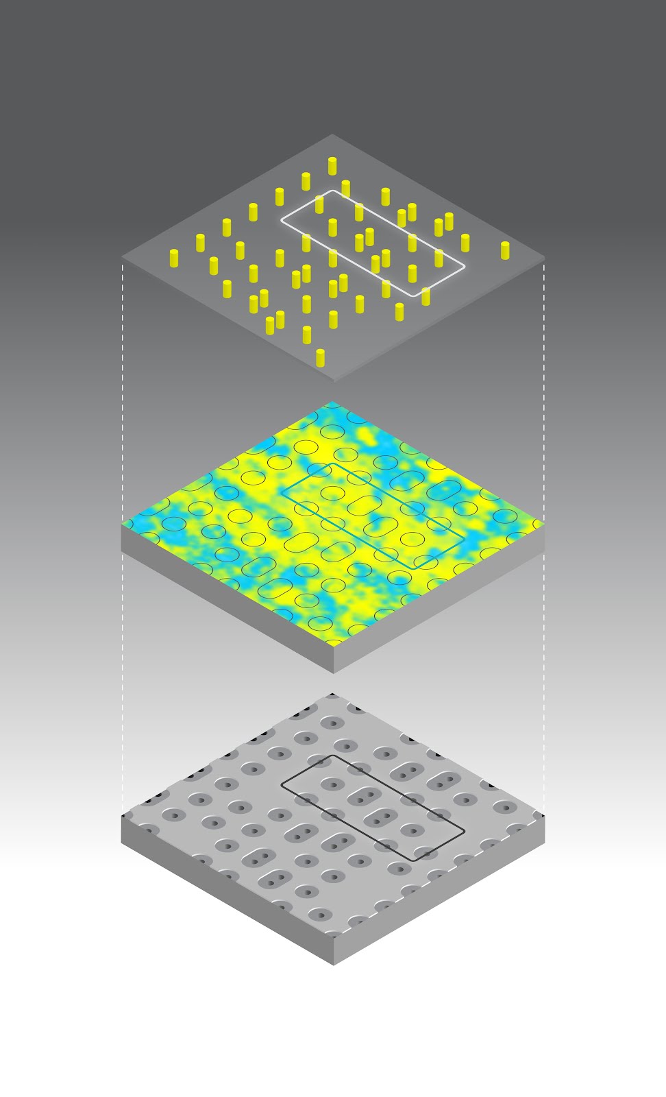
Here researchers demonstrate the contact hole layout for a 22-nm SRAM (top), using a guiding template created with conventional lithography (middle) resulting in the application of a block copolymer to self-assemble the circuit's contact pattern (bottom).
SOURCE: Stanford University
Here is what EETimes says about directed self assembly: A novel self-assembly technique previously demonstrated only in the lab for regular test patterns, has been perfected for creating the irregular patterns necessary to fabricate real semiconductors down to 14-nanometers, according to researchers funded by Semiconductor Research Corp. (SRC).
By solving one of the outstanding lithographic problems facing further scaling—the tiny contact holes that connect semiconductors to their substrate—researchers at Stanford University have demonstrated working circuits at 22-nanometer and a clear path to 14-nanometers, as well as a bee-line on the chemistry developments needed to scale to single digit sizes.
Further Reading
